
Converting bread board or soldered board to a printed circuit board has many benefits and a few downsides.
Advantages
- Professional looking product
- No ugly wires all over the place
- Can be replicated many times
- Can be the size and shape of your choice
Disadvantages
- Usually have to order more than one board per design
- Can be expensive for one board
- If you get the design wrong the board could be scrap.
- Can take a week or so to get the board
- Shipping costs can be more than the price of the board (to Me in Australia)
Software for designing a custom PCB
There are a number of programs to create PBC's. I found that almost all fabrication companies accept Eagle Gerber files. So I used Eagle and there is a free version.
Download Eagle form http://www.cadsoftusa.com/download-eagle/
Eagle free version limitations are listed here http://www.cadsoftusa.com/download-eagle/freeware/ but here is the basics
- The usable board area is limited to 100 x 80 mm (4 x 3.2 inches).
- Only two signal layers can be used (Top and Bottom).
- The schematic editor can only create two sheets.
- Support is only available via email or through our forum (no fax or phone support).
- Use is limited to non-profit applications or evaluation purposes.
Just download the software and install then click the freeware license option.
How to use Eagle
First create a new project. File -> New Project and rename it to a name of your choice.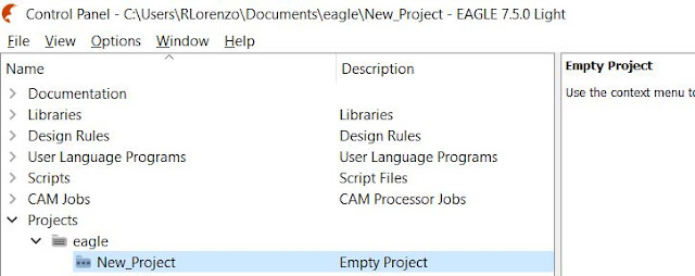

Eagle Libraries
Next you will probably need to upload some libraries for the device that you are using.
A good start is Sparkfun Libraries https://github.com/sparkfun/SparkFun-Eagle-Libraries
Then for specific devices there are a lot available on Element 14 see below screen shot

There are a lot of manufacturer Eagle libraries to down load but not all each device that has a library will have link like the ones I highlighted in green boxes.
Building a Schematic
Once you have some Items you can start to build the schematic. Right click on the project and select New->Schematic

Then minimize and go back to the main Eagle control panel and expand the libraries until you find the item you require and right click Add to Schematic.

The drawing shows the device schematic view on the left and physical view. Below the drawings is a list of connection types usually through hole and surface mount versions of the same device.
Add all the items you require then connect the items together on the Schematic. This takes some time and you should be careful to get it right. Right click gives you options and you can label wire connections. The net tool is the easiest way to connect items as you can then re-route them as required.

I recommend using headers to connect external items like LCD screens, sensors etc. This helps if you need to change connections or replace items and saves the need to re-soldering everything.

Then check the connections with the ERC (Electrical Rule Check) tool the ERC errors will be shown. If you are happy with an error just approve it and the error will be ignored or fix the issue. I did not have a use for all the inputs one 74HC165N chip so I left them unconnected and approved these errors.
PCB layout and wiring
Once the schematic is ready change to board view by clicking on the button from the schematic this will generate the basic PCB board and dump all the components on the page.

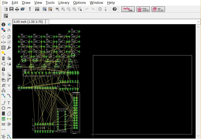
Move each item on to the outlined PCB. This process is a lot of trial and error so just do your best to get everything lined up where you think it will work best. Don't worry about the wiring lines the will be done automatically latter.
To move items click on the cross then move them into position right click will rotate an item if required.

Check the layout with the ERC and fix or approve any errors.
If you want wider solder traces than standard or bigger pads change settings in the DRC (Design Rules Check). The DRC will check that items are not too close together and general layout of the board. Once you have everything how you want it, use the autorouter to run all the wires. This can take some time.

Once finished check the layout. You will probably want to reduce Vias by moving and rotating items. A via is where the connection has go Via another PCB layer to get to its destination. This below example shows some of the 75 vias that is not good.

Then move items around and find the best layout you can taking into account of mounting screws and connections. Here is the same PCB design with a better layout and just 4 vias.

I recommend using headers to connect things like LCD screens, sensors etc this means you can work on or replace the board without re-soldering everything each time. You can see that I have a header for sensor inputs, relay outputs, LCD screen, keypad, real time clock and a big one in the middle for the Raspberry PI.
Creating Gerber Files
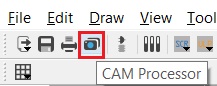
To get a board built you will need Gerber files to send to the company that builds the boards. From the Board view click the CAM processor button.
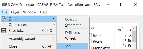
Then from the dialog select File->Open->Job and select the gerb274x.cam
Create a folder to store the gerber files then Click on the File button on each tab and select the new folder (I add a gerber folder under the project folder)

Check the path has changed on each tab. Click the Process Job button

Then do the same process but use the excellon.cam job and put the file in the same folder.
This will create a file for drill holes that some board manufacturers require

The files should look like the below

Now all you need to do is go to a PCB manufacturer and get your board built.
I have used http://www.seeedstudio.com/service/index.php?r=pcb the price was reasonable and they delivered the boards in about a week to Australia. I used a 2 layer board 10 cm x 10 cm there is a minimum order of 5 boards. In the US and Europe there is more choice of PCB manufacturers so you are likely to get a good price locally.
My custom PCB from .Seeed Studio

Here is the board almost fully populated with components.

Thank you for reading and I hope this information helps you build the board of your dreams.
This comment has been removed by a blog administrator.
ReplyDeleteHand wired board assembling is amazing for me which I learnt from here. prototype pcb assembly
ReplyDeleteStating the advantages and disadvantages of converting bread board or soldered board to a printed circuit board is a practical help for those interested in Custom Software Australia
ReplyDeletebased individuals since shipping cost can be a great factor.
Thanks for sharing like this content. I really appreciate sharing your post. and also you can go through this site and read the interesting thing Top PCB Design Companies - 2018
ReplyDeleteRaspberry Pi is a technological marvel adopting the latest innovations of the Printed Circuit Board. I would love to make a Custom Raspberry Pi by modifying existing PCBs. Your blog motivates me to do the same.
ReplyDelete